In the previous article of PCB design we got familiar with types of printed circuit boards with the technical requirements. In this article we will explore the important design elements considerations. These design considerations are related to design of a layout. A layout is a process of designing a structure of the PCB with the help software tools.
Important Design Considerations:-
The design specifications which a PCB designer should take into considerations are as follows-
1) Type of circuits:-
The type of circuit refers to the analog, digital or mixed.
a) Analog Circuit- Circuits which operate on continuous valued signals which are difficult to design due to less flexibility. Components such as transistor, diode capacitor, inductor, resistor forms an analog circuit.
b) Digital Circuit- Circuits which operate on signals existing two levels i.e. 0’s and 1’s with more flexibility and less susceptible to noise. Component such as logic gates.
c) Mixed Circuit- Mixed circuit is any integrated circuit that has both analog circuit and digital circuit characteristics. Components such as micro controllers, micro-chips, etc.
2) Board Size:-
- During the designing of a layout, it is good practice to provide for a 5 to 10 percent area for any modification which may be required on the board. While working on the board size, location based constraints of following components must be considered Connectors, Control or adjusting devices such as potentiometer.
- While calculating board size, following points need to be considered
- Locating holes for assembly:- The preferred diameter of holes is 3.175 mm. Their position is usually close to the longest edge of the board. Their center should be at least 1.5 times the hole diameter from the edge of the board.
- Safety areas need to be provided around the fixing holes, keeping in view the size of the washers and screws.
- Usually a 2-5 mm safety strip is provided along all edges. It is necessary as trimming of the board could cause de-lamination of copper areas too close to the edge.
It is generally not possible to prescribe a universally applicable standard for the board size, though the ideal board size should be neither very large nor very small.
3) Number of layers:-
The number of layers in a PCB depend on the application covered by the user and the type of PCB used. As we have already seen the types and layers in the 1st article of PCB.
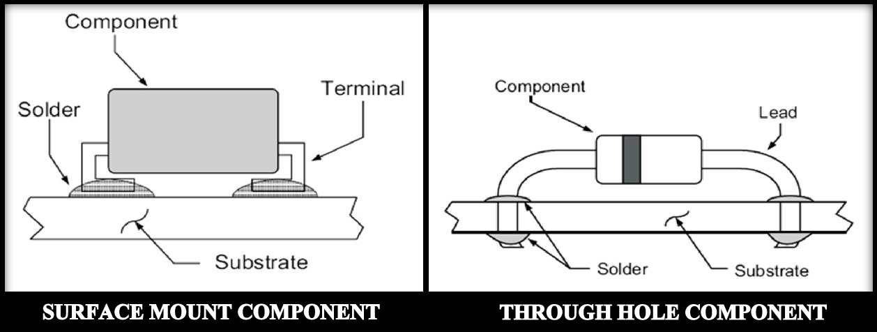
4) Pad:-
- Pad’s are in all sorts of shapes and size. They can be through hole or SMD but they all follow the same guidelines
- Through hole are used for leaded components like resistors and capacitors round.
- Dual in packages components like IC’s are better with the oval shape through hole pad.
- Surface mount (mount) components are better to rectangle shape.
5) Conductor Dimensions:-
Conductor dimensions are determined by component packing density.
The copper printed tracks on PCB have finite resistance which introduces a voltage drop proportional to the current flowing in that particular conductor.
The resistance depends upon the specific resistivity of copper, which is 1.724 X 10⁻⁶ Ohm cm at 20oC.
Let us try to determine the resistance of 1 mm wide copper conductor per cm of length. (With copper foil thickness 35 micro-meter)
R = p*L/A.
p= Resistivity.
L= Conductor length (cm).
A= Area of the conductor.
So, L = 1 cm, A = 35 X 10-4 X 0.1 cm2, R = 5 m Ohms.
This shows, that a 1 mm wide conductor of 1 cm length for standard copper foil of 35 um thickness is 5 m Ohms. So, if we make it as 0.5 mm wide then, R = 9.85 m Ohm.
We can say that, half the conductor width gives double resistance (i.e. high value of resistance). The resistivity factor of the material is valid for 20oC and it will rise with temperature. The specific resistivity of copper at 25oC is 1.78X10⁻⁶

Conductor width selection-
Let us assume that 8 Amp current is flowing, 35 uM copper clad width and temperature rise is 300 above room temperature.
Procedure:-
a) Find 8 Amp in the left top scale.
b) Follow the 8 Amp line to intersect the 300 graph line
c) Follow the vertical line from point down to intersect the 35 uM copper graph line.
d) Draw a horizontal line to the left from that intersection to find the minimum conductor width, which, in this case, is 2.6 mm
6) Supply and ground conductor:-
The width of the conductors and their layout plays an important role in imparting the stability to the circuit voltages. In some cases, resistive losses in these conductors may result in unstable supply voltage and ground system. When many supply voltages are used in the circuit, it must be insured that the ground conductor has the capacity to carry the combined load under the worst conditions.
Conductor width of ground line > Conductor width of supply line
7) Wire Parastics:-
Wire parasitic’s are basic electrical elements used for construction of a system on the PCB. The elements are resistors, capacitors, inductors. The value of these elements must be computed while designing the circuit so that their effect on circuit performance can be predicted