Earlier, we have discussed most of the important considerations and points required for the PCB design in previous article. Now let us have a look at some points which have importance for the layout design like the schematic diagram, artwork, polyester filming and layout printing. These mentioned steps are involved before actual layout design. We will discuss them first and then the PCB design steps.
Schematic Diagram:-
A schematic diagram is a graphical representation of interconnects of various electronic, electrical components of an equipment. The schematic is the first step in an electronic circuit design, because it displays and identifies the devices or components required that make up the equipment.
The schematic diagram shows various components by means of symbols which are so arranged that they show the working of the circuit in a appropriate way. The symbols of components are usually governed by various standards.
Artwork:-
The components and connections in the PCB layout are derived from the circuit diagram, and physically place and routed by the designer to get the best results in terms of the board size and its manufacturing ability. The final physical form of the circuit and labeling details are finalized as the layout is completed which is defined by the PCB layout. The artwork process consists of routing for proper connections of signals.
Polyester film:-
The polyester film is used as a printing material for the PCB layout. The designed artwork is printed on the film. It is very important to use a film with appropriate thickness i.e. if a very thick film is used then it can lead to slight distortion in the layout to be printed.
Printing devices:
The printing device consists of laser printers, pen plotters, manual markers, inkjet printers. But Pen plotters and manual markers are not used now, as these were traditional methods, the biggest disadvantage of using pen plotters and manual markers is that they consume lot of time, which is improper and inappropriate for mass production in any industry. It may lead to drastic financial losses.
Now, let’s get on with the traditional method of PCB design, one by one.
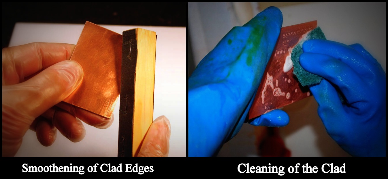
Step 1:
Smooth the edges of the copper clad using a sandpaper or carborundum which may be wrapped around a small piece of soft wood. The copper clad surface has to be cleaned using soft cleansers and scrubs in order for resist to adhere to it properly. After cleaning do not touch the copper surface with bare fingers.
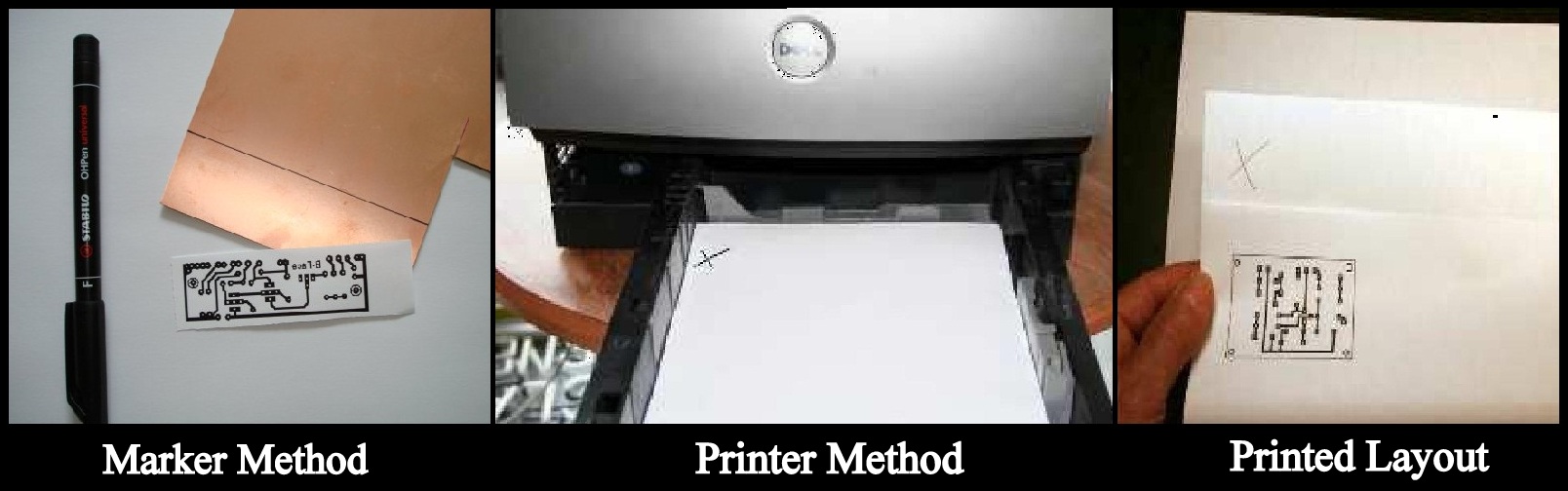
Step 2:-
Now, the clad is ready for receiving the design pattern. Before imprinting on the clad we need to print the pattern to a piece of plain paper. As we can see in the figure below that we get a printed layout on the paper. Even we can draw the layout using a marker on a piece of paper as shown below.
Step 3:-
Now you can use this same sheet as a “carrier” for a small piece of the transfer film i.e. polyester film.
Cut out a piece of film that is slightly larger than the printed image layout. Need to press and lay this down carefully over the printed page with the dull (emulsion) side facing up. Without bare fingers press the film down gently with a clean sheet of paper for a good adhesion.

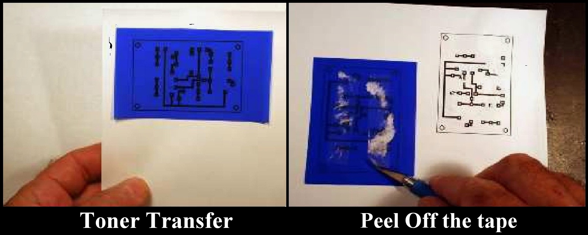
Step 4:-
Now be ready to print for real. Load the sheet into the printer paper and print it. If everything is right, we have a toner transfer. Gently lift the transfer off the carrier sheet and carefully peel away the tape.
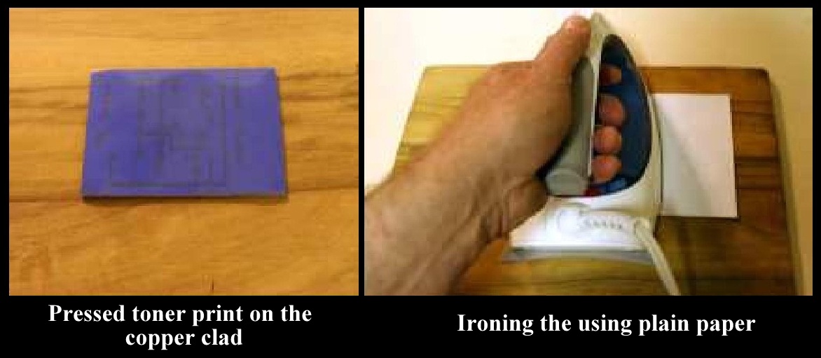
Step 5:-
Next step is ironing so use a wooden board which sets a hard base below the clad. Set the temperature control of the iron. Use a piece of plain paper between the toner transfer and the iron it for reducing the friction of the clad. Slowly, back and forth, and it doesn’t take much pressure. Small boards don’t usually need more than 90 seconds.
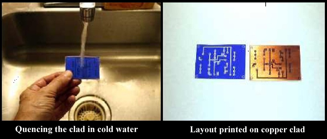
Step 6:-
Quench the board under cold running water to bring it back to room temperature, and peel the film away gently. If pattern didn’t come out well then we need to remove the pattern by rubbing with a acetone and do the transfer again. As shown in figure we get the printed copper clad.
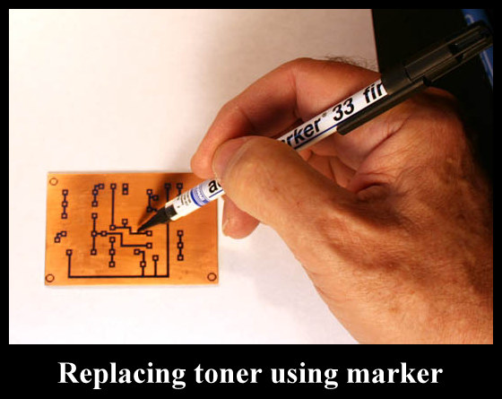
Step 7:-
Replace any missing toner on the board with ink from a permanent black marker. Now we need the ink to dry for a few hours.
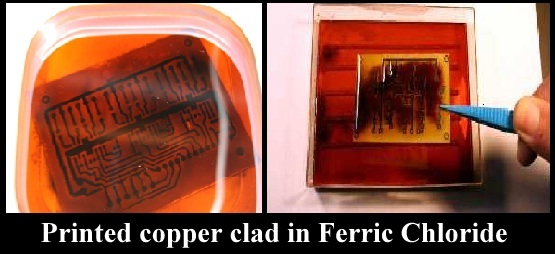
Step 8:-
Once you have the pattern defined on copper, the board is ready to etch. Lay the board in the tray and pour in enough Ferric Chloride to just cover it. Slightly shake the tank after few minutes, and pull out the board periodically to check the etching progress.
Step 9:-
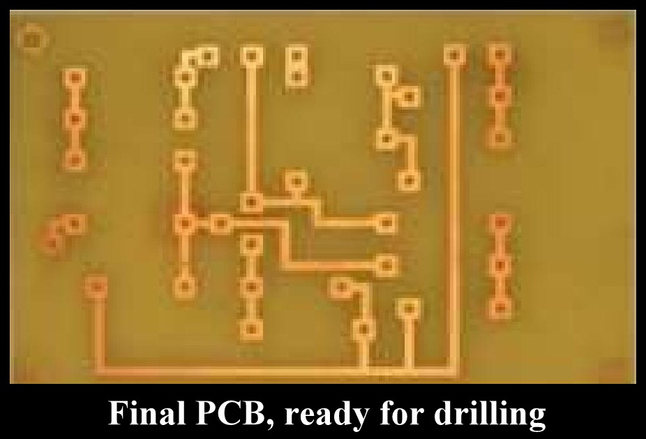
When the board is fully etched, rinse it thoroughly in running cold water. Strip the resist with acetone. The board is ready to drill.